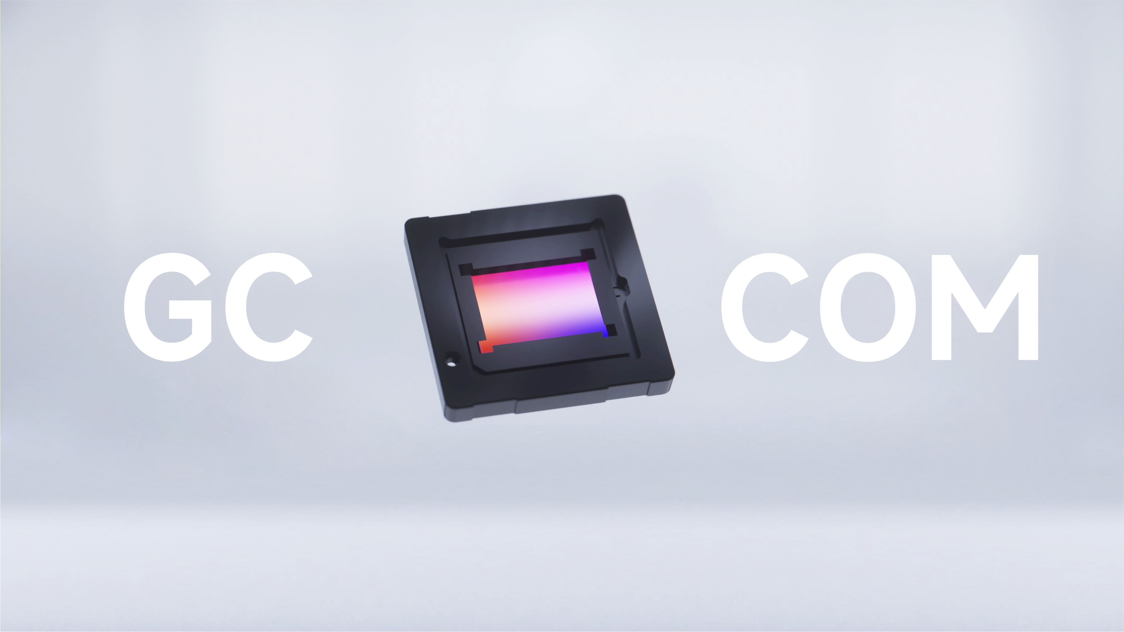
The performance of an image sensor relies not only on its design and manufacturing but also on the packaging technology.
CIS packaging is particularly challenging, as any particle in the environment that drops on the sensor surface during the process can cause a significant affect on the final image quality. GalaxyCore’s COM (Chip on Module) packaging technology has revolutionized traditional CSP (Chip Scale Package) and COB (Chip on Board) methods, enhancing the performance, reliability, and applicability of the optical system of camera modules.
Birth of the COM Packaging
Before the advent of COM packaging, CSP and COB were the predominant packaging choices for CIS. CSP places a layer of glass on the sensor to prevent dust. However, the glass also reflects some light, thus degrading image quality. COB requires an exceptionally demanding environment, typically a Class 100 clean room.
Is there an alternative? GalaxyCore’s technical team developed an innovative solution by directly suspending gold wire to serve as pins. In the fantastic microscopic realm, the short gold wire becomes hard and elastic, which can used directly as pins.
At GalaxyCore’s Class 100 clean rooms in the packaging and testing factory in Jiashan City, Zhejiang Province, a fully-automated high-precision equipment bonds the gold wire to the image sensor with exacting accuracy. The sensor is then mounted on a filter base, and the other end of the gold wire is suspended as the pin. The pin is subsequently soldered by the camera module manufacturer to the FPCB. When assembled with a lens and the actuator, a complete camera module can be formed.
 We were pleasantly surprised to discover that the performance and reliability of the COM packaging are on par with, or even exceed, those of high-end COB packaging.
Click the video below to see how GalaxyCore’s COM packaging delivers system-level enhancements to camera modules.
For more information, please visit GalaxyCore's official X and Youtube accounts.
Three Advantages for System-level Improvement
1、Enhanced Optical System Performance
The COM packaging notably enhances the optical system performance of camera modules. In the COB packaging, the chip is directly mounted on the FPCB. However, the FPCB is prone to deformation during production, which may lead to the tilt of the optical axis and further affect the image quality.
In GalaxyCore’s COM packaging, both the chip and lens use the filter base as the benchmark, thus mitigating the optical axis tilt caused by FPCB deformation. This significantly improves the edge resolution of images, especially in large aperture and high-pixel camera modules.

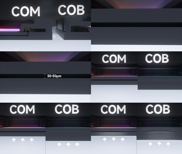
Compared to the COB packaging, where the chip is directly mounted on the FPCB, the COM chip is mounted on a filter base. This forms a natural confined space that effectively prevents moving particle from contaminating the light-sensitive surface of the chip.

< COM Confined Space Structure>
2. Improved Module Reliability and Flexibility
In the COM packaging, due to a certain distance between the chip and the FPCB, the camera module is subject to greater back pressure, thus improving the reliability and durability of the module.
In the COB packaging, the CIS directly mounted on the FPCB is more sensitive to the back pressure, and the SFR (i.e. image resolution) is more likely to be affected. By contrast, in the COM packaging, the CIS chip is relatively isolated and suspended, making it hard for the back pressure to directly act on the CIS chip. As such, a better image resolution can be achieved.
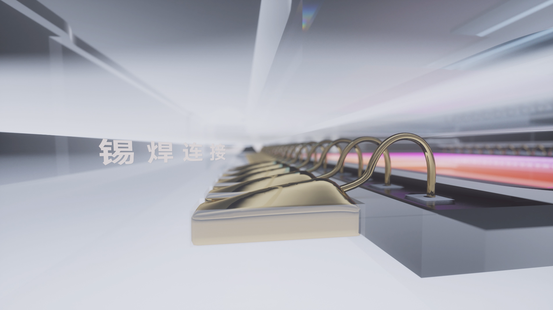
Different from the COB packaging, the COM packaging connects the chip pins and pads through soldering. This solution reduces the material requirements for the FPCB and further enhances its adaptability and flexibility.
3. Minimized Module
In the COM packaging, FPCB can be hollowed out to allow the chip to sink into it. Compared to the COB packaging with direct mounting of chip on the FPCB or reinforcement of steel sheets, the COM solution can control the back pressure more effectively and reduce the requirements for steel sheet thickness. This enhances the height advantage of the overall packaging module, to meet cell phones’ stringent requirements for space. This advantage is more notable in devices seeking thin and light designs.
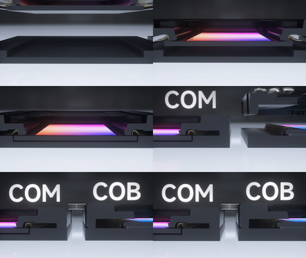
GalaxyCore’s COM packaging ensures both high performance and reliability for the optical system while simplifying the subsequent production processes for module manufacturers. This method reduces the dependence on dust-free environments and enhances quality, yield, and efficiency. With the mass production of COM chips and further application of this technology, it will deliver improved imaging performance across a broader range of end products.

